Technologies
Elliptika
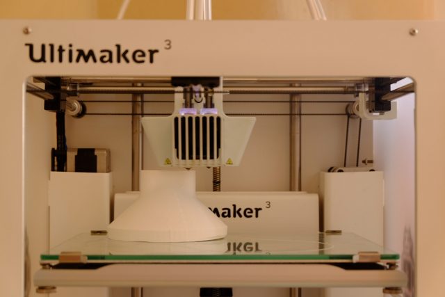
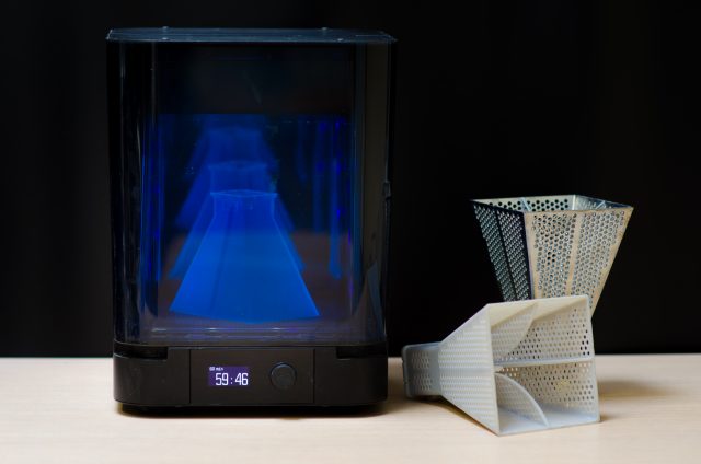
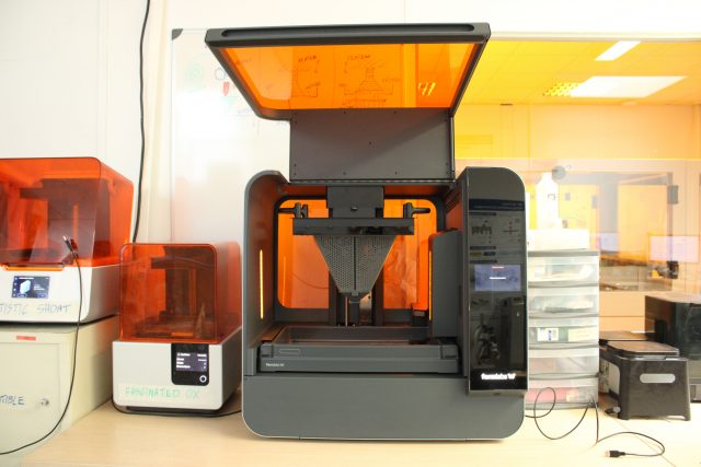
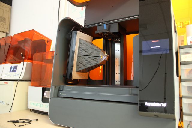
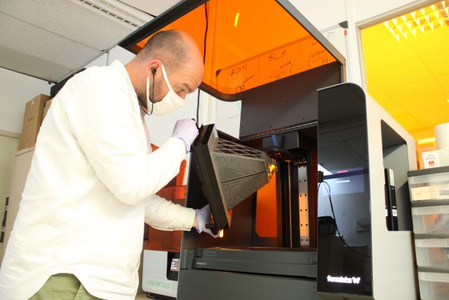
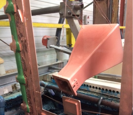
Within the group in Brest, the company has all the means of production. Internally, we have a sufficient machine park of 3D printers to be autonomous in the production of our 3D printing components. In addition, Protecno allows us to control the manufacture of printed circuits and TE2M the realization by machining or sheet metal.
Elliptika also has expertise in the production of printed circuits, relying in particular on the know-how of PROTECNO, also a subsidiary of the GTID group.
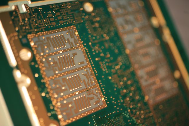
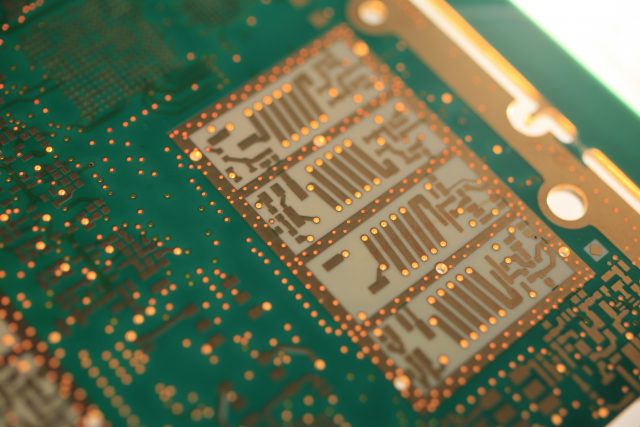
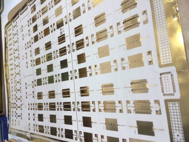
PROTECNO is a specialist in complex printed circuit boards from prototype to medium series produced within short deadlines. Its production site meets the demands of the technological PCB market for high added value sectors such as aeronautics, defense, research, connected objects or electronic subcontracting.
PCB manufacturing offered by PROTECNO:
– Multilayer PCBs (50%)
Power type (planar transformers, backplane board)
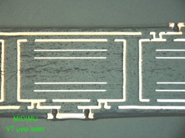
HDI sequential digital type with microvias
– Flex-rigid (25%) flexible multi-layer PCBs up to 8 levels.
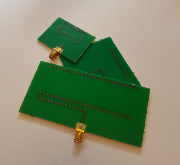
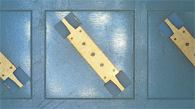
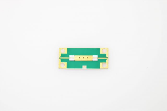
– PCBs with multilayer microwave applications (25%) with antenna functions and planar filters integrated on the circuit
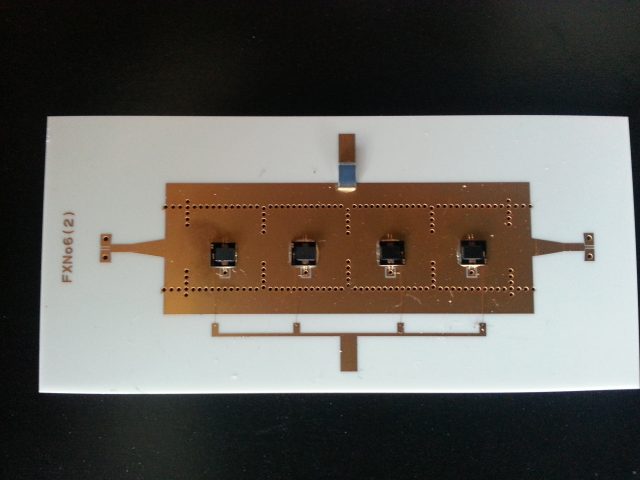
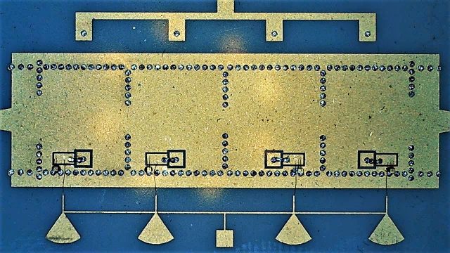
We also have great expertise in SIW technology. The technique consists of combining planar and volume technology. It was introduced with the idea of getting the best out of each: compactness, cost, compatibility and ease of construction for planar solutions and electrical performance for volume solutions. This technique consists in delimiting a cavity filled with dielectric in a planar substrate. To do this, the upper and lower electrical walls are obtained using conventional metallization processes and the side faces are for their part made through one or more rows of metallized holes.

